

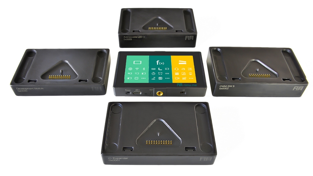
while also supporting other special modules. The specific choice of modules mainly depends on the required functionalities, costs, protection levels, and different application scenarios.
| R01 | R02 | R03 | R04 | R05 | R06 | R07 | R08 | R09 | R10 | R11 | |
|---|---|---|---|---|---|---|---|---|---|---|---|
| C1 | 3.3v¹ | IO41 | IO42 | IO09 | IO40 | IO06 | IO05 | IO02 | IO01 | 5V² | GND |
| C2 | GND | IO20 | IO19 | IO12⁴ | IO44 | IO43 | IO13 | IO14 | IO45 | IO04 | 5V³ |


| R1 | R2 | R3 | R4 | R5 | R6 | R7 | R8 | R9 | R10 | R11 | |
|---|---|---|---|---|---|---|---|---|---|---|---|
| C1 | 3.3v | IO41 | IO42 | IO09 | IO40 | IO06 | IO05 | IO02 | IO01 | 5V | GND |
| C2 | GND | IO20 | IO19 | IO12 | IO44 | IO43 | IO13 | IO14 | IO45 | IO04 | 5V |
| I2C | – | SCL | SDA | – | – | – | – | – | – | – | – |
| I2C | – | – | – | – | – | – | – | – | – | – | – |
| R1 | R2 | R3 | R4 | R5 | R6 | R7 | R8 | R9 | R10 | R11 | |
|---|---|---|---|---|---|---|---|---|---|---|---|
| C1 | 3.3v | IO41 | IO42 | IO09 | IO40 | IO06 | IO05 | IO02 | IO01 | 5V | GND |
| C2 | GND | IO20 | IO19 | IO12 | IO44 | IO43 | IO13 | IO14 | IO45 | IO04 | 5V |
| UART | – | – | – | – | – | – | RST | RX | TX | – | – |
| UART | – | – | – | – | – | – | – | – | – | – | – |

| R1 | R2 | R3 | R4 | R5 | R6 | R7 | R8 | R9 | R10 | R11 | |
|---|---|---|---|---|---|---|---|---|---|---|---|
| C1 | 3.3V | IO41 | IO42 | IO09 | IO40 | IO06 | IO05 | IO02 | IO01 | 5V | GND |
| C2 | GND | IO20 | IO19 | IO12 | IO44 | IO43 | IO13 | IO14 | IO45 | IO04 | 5V |
| USB-HID | – | – | – | – | – | – | – | – | – | – | – |
| USB-HID | – | D+ | D- | – | – | – | – | – | – | – | – |
| R1 | R2 | R3 | R4 | R5 | R6 | R7 | R8 | R9 | R10 | R11 | |
|---|---|---|---|---|---|---|---|---|---|---|---|
| C1 | 3.3V | IO41 | IO42 | IO09 | IO40 | IO06 | IO05 | IO02 | IO01 | 5V | GND |
| C2 | GND | IO20 | IO19 | IO12 | IO44 | IO43 | IO13 | IO14 | IO45 | IO04 | 5V |
| USB-UART | – | – | – | – | – | – | – | – | – | – | – |
| USB-UART | – | – | – | – | RX | TX | – | – | – | – | – |
| R1 | R2 | R3 | R4 | R5 | R6 | R7 | R8 | R9 | R10 | R11 | |
|---|---|---|---|---|---|---|---|---|---|---|---|
| C1 | 3.3V | IO41 | IO42 | IO09 | IO40 | IO06 | IO05 | IO02 | IO01 | 5V | GND |
| C2 | GND | IO20 | IO19 | IO12 | IO44 | IO43 | IO13 | IO14 | IO45 | IO04 | 5V |
| SPI | – | – | – | SCK | MOSI | MISO | – | – | – | – | – |
| SPI | – | – | – | – | – | – | – | – | – | – | – |
| R1 | R2 | R3 | R4 | R5 | R6 | R7 | R8 | R9 | R10 | R11 | |
|---|---|---|---|---|---|---|---|---|---|---|---|
| C1 | 3.3V | IO41 | IO42 | IO09 | IO40 | IO06 | IO05 | IO02 | IO01 | 5V | GND |
| C2 | GND | IO20 | IO19 | IO12 | IO44 | IO43 | IO13 | IO14 | IO45 | IO04 | 5V |
| INTERRUPT | – | – | – | – | – | – | – | – | – | – | – |
| INTERRUPT | – | – | – | INT | – | – | – | – | – | – | – |
| R1 | R2 | R3 | R4 | R5 | R6 | R7 | R8 | R9 | R10 | R11 | |
|---|---|---|---|---|---|---|---|---|---|---|---|
| C1 | 3.3V | IO41 | IO42 | IO09 | IO40 | IO06 | IO05 | IO02 | IO01 | 5V | GND |
| C2 | GND | IO20 | IO19 | IO12 | IO44 | IO43 | IO13 | IO14 | IO45 | IO04 | 5V |
| Non-protocol Pin | – | – | – | – | – | – | Y | – | – | – | – |
| Non-protocol Pin | – | – | – | – | – | – | Y | Y | Y | Y | – |
| Address | Function | R/W | Comments |
|---|---|---|---|
0x00/02 |
Module Number | R | |
0x01/03 |
Module Number | R | |
0x04 |
Total Number of Registers | R | |
0x05 |
Hardware Version | R | |
0x06 |
Software Version | R | |
0x07 |
Functions Used | R | |
0x08 |
Checksum | R | |
0x09/0A/0B/0C/0D/0E |
Reversed | R | |
0x0E |
New data flag | R/W | |
0x10->0x2F |
Module Name | R | |
0x30 |
PIN-01 Status | R | |
0x31 |
PIN-02 Status | R | |
0x32 |
PIN-04 Status | R | |
0x33 |
PIN-05 Status | R | |
0x34 |
PIN-06 Status | R | |
0x35 |
PIN-09 Status | R | |
0x36 |
PIN-12 Status | R | |
0x37 |
PIN-13 Status | R | |
0x38 |
PIN-14 Status | R | |
0x39 |
PIN-19 Status | R | |
0x3A |
PIN-20 Status | R | |
0x3B |
PIN-40 Status | R | |
0x3C |
PIN-41 Status | R | |
0x3D |
PIN-42 Status | R | |
0x3E |
PIN-43 Status | R | |
0x3F |
PIN-44 Status | R | |
0x40 |
PIN-45 Status | R | |
0x41 |
Interrupt Flag | R/W |
Each module has a different and unique number, ranging from 0x0001 to 0xFFFF. Different versions of the same module use the same number. The hardware version is used to distinguish between hardware. To ensure the correct identification of the module, the system stores the number twice to prevent the I2C from connecting to other devices.
| 0x00/0x02 | B7 | B6 | B5 | B4 | B3 | B2 | B1 | B0 |
|---|---|---|---|---|---|---|---|---|
| High 8 Bits | 0 | 0 | 0 | 0 | 0 | 0 | 0 | 0 |
| 0x01/0x03 | B7 | B6 | B5 | B4 | B3 | B2 | B1 | B0 |
|---|---|---|---|---|---|---|---|---|
| Low 8 Bits | 0 | 0 | 0 | 0 | 0 | 0 | 0 | 0 |
The total number of registers ranges from 0x00 to 0xFF, equal to the number of general registers plus the number of private registers. This total number is stored at address 0x04.
| 0x04 | B7 | B6 | B5 | B4 | B3 | B2 | B1 | B0 |
|---|---|---|---|---|---|---|---|---|
| Val | 0 | 0 | 0 | 0 | 0 | 0 | 0 | 0 |
The hardware version of the module increments among modules with the same functionality, ranging from 1 to 255, with the first version being 1. This version information is stored at address 0x05.
| 0x05 | B7 | B6 | B5 | B4 | B3 | B2 | B1 | B0 |
|---|---|---|---|---|---|---|---|---|
| Val | 0 | 0 | 0 | 0 | 0 | 0 | 0 | 0 |
The software version of the module can be upgraded via the host, ranging from 1 to 255, with the first version being 1. This version information is stored at address 0x06.
Firmware updates do not modify the data in the EEPROM, but during module initialization, the old data may be used, which could lead to data errors. The software version also serves to determine whether data should be read from the EEPROM to initialize the module.
| 0x06 | B7 | B6 | B5 | B4 | B3 | B2 | B1 | B0 |
|---|---|---|---|---|---|---|---|---|
| Val | 0 | 0 | 0 | 0 | 0 | 0 | 0 | 0 |
Different modules have different functionalities, so the required communication protocols also vary. The protocol used by this module is stored at register 0x07 for the host to identify.
Each bit represents the communication protocol used by the module, with 0 indicating not in use and 1 indicating currently in use. All modules support the I2C protocol.
| 0x07 | B7 | B6 | B5 | B4 | B3 | B2 | B1 | B0 |
|---|---|---|---|---|---|---|---|---|
| Protocal | – | – | UPGRADE | USB-HID | USB-UART | INTERRUPT | UART | SPI |
The checksum value is the low eight bits of the sum from 0x00 to 0x07. This checksum is stored at address 0x08.
| 0x08 | B7 | B6 | B5 | B4 | B3 | B2 | B1 | B0 |
|---|---|---|---|---|---|---|---|---|
| Val | 0 | 0 | 0 | 0 | 0 | 0 | 0 | 0 |
The address range 0x09 – 0x0E is reserved, unused, and has a value of 0.
If the module has new data, this value needs to be incremented. When the host polls, it first reads this register. If the value is not 0, it continues to read other registers and then clears it. This value is stored at address 0x0F. If the value of this register is large, the host needs to shorten the polling interval.
| 0x0F | B7 | B6 | B5 | B4 | B3 | B2 | B1 | B0 |
|---|---|---|---|---|---|---|---|---|
| Val | 0 | 0 | 0 | 0 | 0 | 0 | 0 | 0 |
The module name must be unique and start with "WF1-", with a maximum of 32 characters following it, consisting only of letters, numbers, or hyphens (-). The module name is stored in the register range 0x10 – 0x2F.
After confirming the protocol used by the module, the pin status will be initialized when the module is powered on. The pin status is not saved to EEPROM but is initialized by the program in the registers. There are four definitions for the pins, representing different statuses. A total of 2 bits are used to represent different statuses, BIT0 and BIT1, with other bits reserved. The specifics are as follows:
| 0x30 | B7 | B6 | B5 | B4 | B3 | B2 | B1 | B0 |
|---|---|---|---|---|---|---|---|---|
| Val | – | – | – | – | – | – | IO | xx |
The steps to set the pin status are as follows:
This pin is not connected to any lines of the module and can be considered a useless pin for this module. These pins cannot be modified by the host. Specific cases include:
The pin is connected to the module’s lines but is not used by the current module and can be used by other modules. Specific cases include:
This status is modified by the host, and the module needs to save the status of these pins to EEPROM.
The pins used on the module cannot be modified by the host. Specific cases include:
If the module uses certain fixed pins, their status must be set to 0b11 and cannot be modified by the host.
| address | Pin # | Protocol | Name | Priority |
|---|---|---|---|---|
| 0x30 | IO01 | UART/UPGRADE | TX | 1 |
| 0x31 | IO02 | UART/UPGRADE | RX | 1 |
| 0x32 | IO04 | Non-protocol Pin | – | 0 |
| 0x33 | IO05 | UPGRADE | RST | 1 |
| 0x34 | IO06 | SPI | MISO | 2 |
| 0x35 | IO09 | SPI | SCK | 2 |
| 0x36 | IO12 | INTERRUPT | High-Level Triggered | 3 |
| 0x37 | IO13 | Non-protocol Pin | – | 0 |
| 0x38 | IO14 | Non-protocol Pin | – | 0 |
| 0x39 | IO19 | USD-D | D+ | 2 |
| 0x3A | IO20 | USD-D | D- | 2 |
| 0x3B | IO40 | SPI | MOSI | 2 |
| 0x3C | IO41 | I2C | SCL | 3 |
| 0x3D | IO42 | I2C | SDA | 3 |
| 0x3E | IO43 | USB-UART | TX | 2 |
| 0x3F | IO44 | USB-UART | RX | 2 |
| 0x40 | IO45 | Non-protocol Pin | – | 0 |
If the module has information that requires immediate processing by the host, it can notify the host by pulling the interrupt pin high. Since multiple devices share the interrupt, the host needs to read the register values of different modules to quickly determine which module triggered the interrupt. After the host processes this interrupt, it sets this bit to 0, and the module will immediately pull the interrupt pin low. The register address is 0x41.
All modules’ private information registers start from address 0x42.